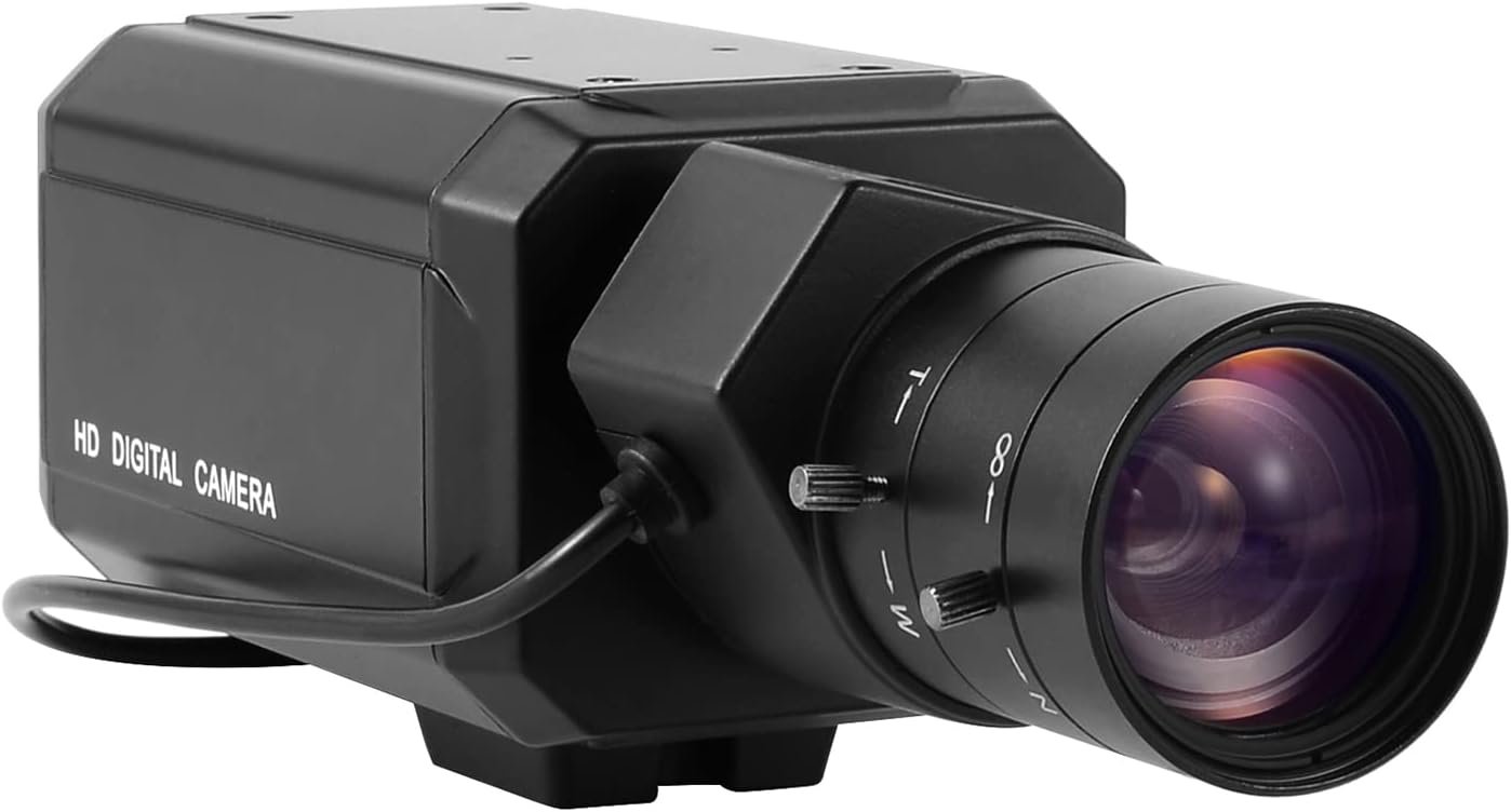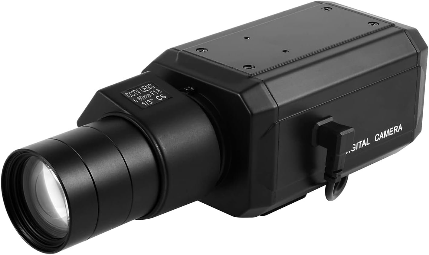
I design customized edge AI cameras end to end — schematic, hardware, embedded Linux, on-device vision, and the connectivity to get results wherever they're needed.
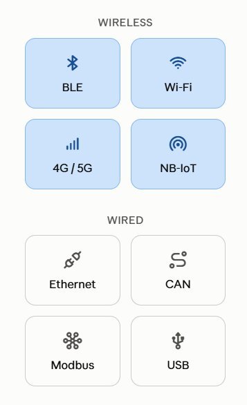
I'm an AI camera engineer based in Seoul. I own the whole lifecycle of a customized edge AI camera — schematic and PCB design, mechanical and enclosure, manufacturing and test, certification, Yocto-based embedded Linux, MCU/PMIC/sensor firmware, camera driver and ISP bring-up, on-device AI implementation, and getting results out over BLE, Wi-Fi, Ethernet, CAN, Modbus, USB, 4G/5G and NB-IoT.
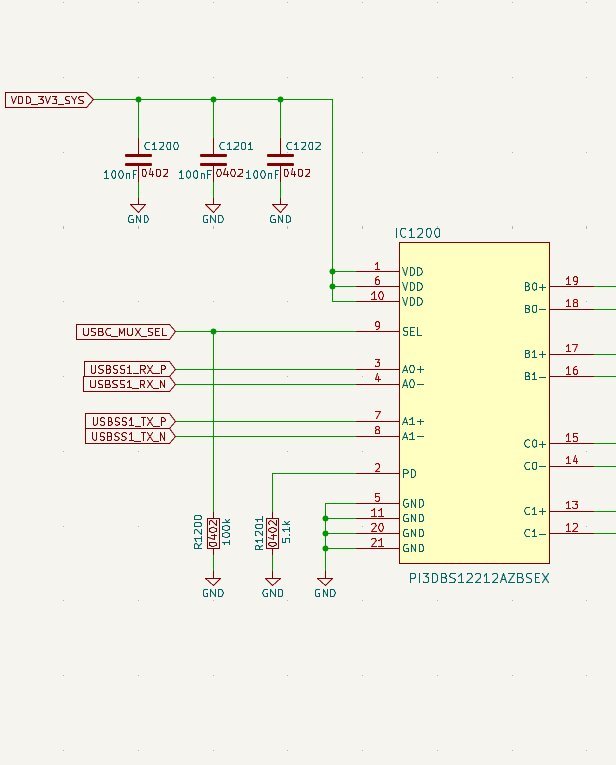
Circuit design and component selection for camera, sensor, power and MCU stages — the electrical foundation everything else builds on.
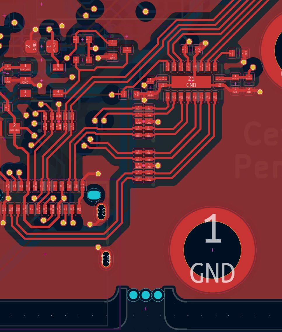
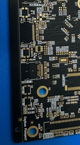
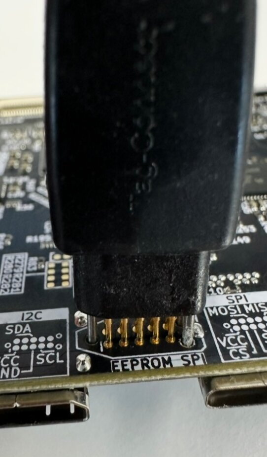
High-speed and mixed-signal board layout, from stack-up planning to routing camera interfaces, power rails and RF sections cleanly.
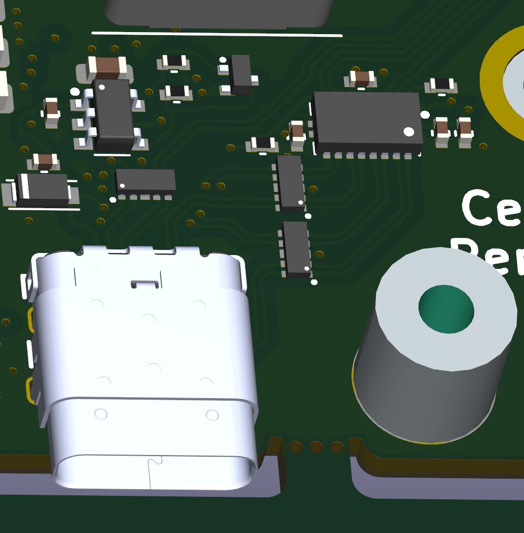
Enclosure and mechanical design — thermal, mounting and environmental sealing that keeps hardware field-ready.
Supporting production runs and functional test, catching hardware issues before they reach the field.
Preparing hardware and documentation for regulatory certification, so products can actually ship.
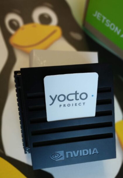
Building and customizing Yocto-based embedded Linux images tailored to the target hardware.
Low-level firmware for MCUs, PMICs and sensor peripherals — the code that keeps hardware alive.
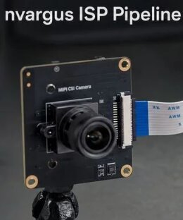
Bringing up camera sensor drivers and tuning the ISP pipeline for clean, usable frames.
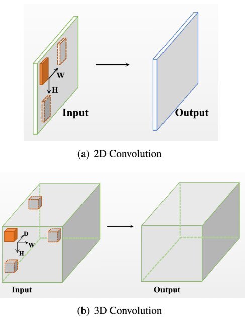
Implementing and optimizing on-device AI detection — from YOLO to Transformer-based models — to run reliably at the edge.
Delivering results over BLE, Wi-Fi, Ethernet, CAN, Modbus, USB, 4G/5G and NB-IoT — whatever the deployment needs.
A camera platform built around what you're actually detecting — sensor, AI model and connectivity chosen per deployment, not a one-size-fits-all box.
Every deployment is different — let's talk about a camera built around your sensors, your model, and your connectivity.
GET IN TOUCH